
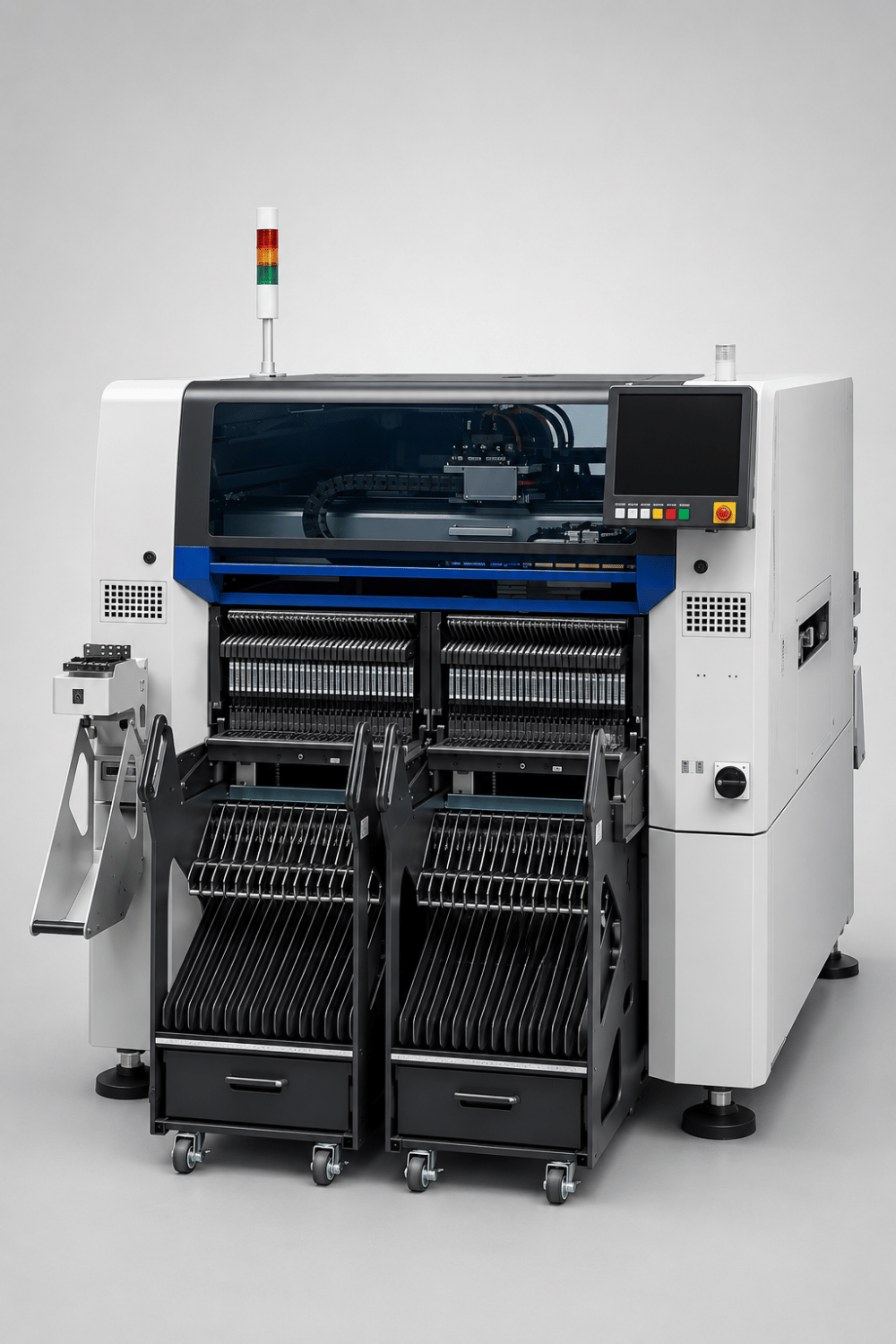
SMT Line
High-speed SMT assembly for fine-pitch components
Capacity 45K CPH

Extreme Thermal Performance
Dissipates intensive heat steadily for high-power semiconductor modules.
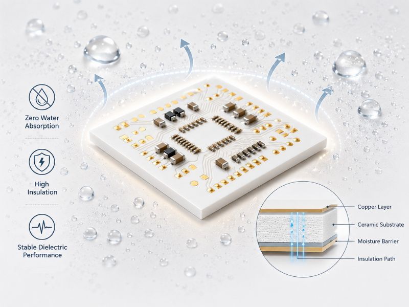
Superior Insulation Stability
Zero water absorption ensures consistent high-voltage insulation performance.
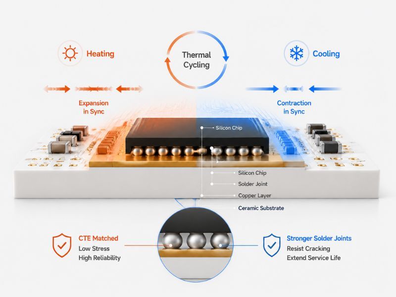
Precision CTE Matching
Silicon-matched expansion rate reduces thermal cycling stress.
Submit your high-power and high-frequency PCB design files, and our team provides precise DFM optimization and custom ceramic PCB manufacturing solutions.
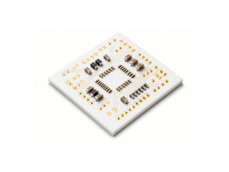
Ceramic PCB is a high-reliability inorganic substrate circuit board, mainly adopting Alumina (Al₂O₃) and Aluminum Nitride (AlN) materials. Different from FR4 and metal core PCBs, it features zero water absorption, ultra-low thermal expansion and excellent high-temperature resistance, breaking the performance limits of organic substrates in extreme working conditions.
Cost-effective 96%/99.6% alumina for conventional high-power scenarios, and high-performance AlN for ultra-high heat flux and high-frequency precision applications.
Inorganic ceramic structure achieves zero water absorption and high dielectric strength, maintaining stable insulation under long-term high temperature and high humidity.
Industry-leading CTE close to silicon chips, effectively reducing solder joint fatigue and cracking during thermal cycling.
Graded alumina and AlN ceramic structures matching different thermal and precision grade requirements.
Cost-effective 96% alumina substrate with mature DBC copper plating. It balances reliable insulation and basic thermal performance for cost-sensitive high-power scenarios.
Ordinary high-power LED lighting, low-medium power industrial power supplies
Extreme performance substrates for high-power, high-frequency and long-lifespan electronic systems.
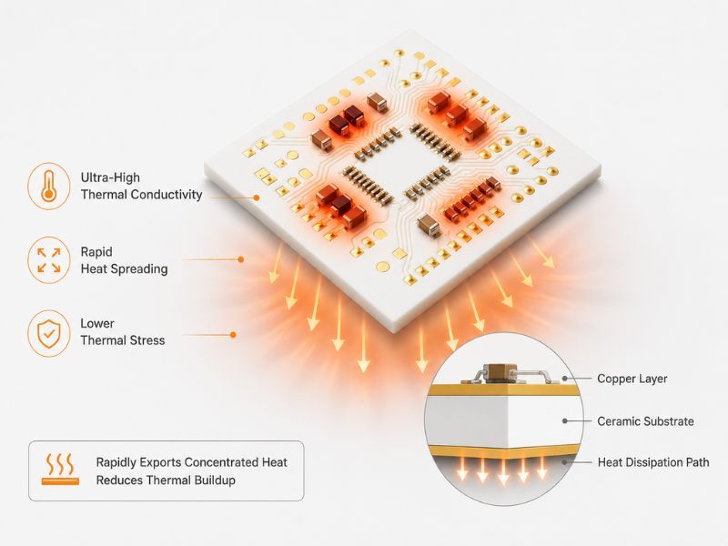
Industry-standard graded parameters for alumina and AlN ceramic PCB, covering general power to ultra-high-precision RF & power applications.
 Capability |  Alumina Ceramic PCB (Al₂O₃) |  AlN Ceramic PCB (Aluminum Nitride) |
|---|---|---|
| Min. trace / space | 4/4 mil (fine line routing) | 3/3 mil (ultra-fine precision routing) |
| Supported Layer Count | 1–4 layers (DBC single substrate) | 1–6 layers (LTCC multi-layer custom) |
| Substrate Thickness | 0.25mm–1.0mm standard thickness | 0.2mm–1.5mm full customization |
| Thermal Conductivity | 24–35 W/(m·K) | 170–230 W/(m·K), 6–8× higher than alumina |
| CTE Thermal Expansion | 4.6–5.5 ppm/°C | 2.6–3.5 ppm/°C, silicon-chip matched |
| Min. Laser Via Size | 0.15mm laser microvia | 0.10mm ultra-fine laser microvia |
| Surface Finishes | Thick Film Silver, ENIG, Copper Plating | High-Precision ENIG, Hard Gold, DPC Copper |
| Typical Applications | High-power LED, industrial power supplies, general semiconductor modules | 5G RF communication, automotive power |
Advanced production equipment supporting stable quality, capacity, and reliable delivery.
High-speed SMT assembly for fine-pitch components
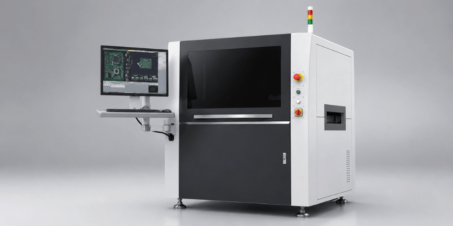
Automated visual inspection for defects
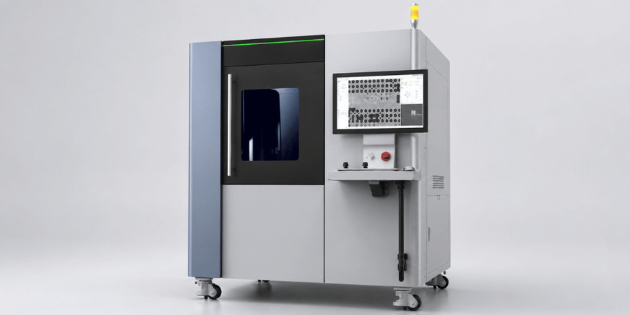
Non-destructive inspection for hidden solder joints
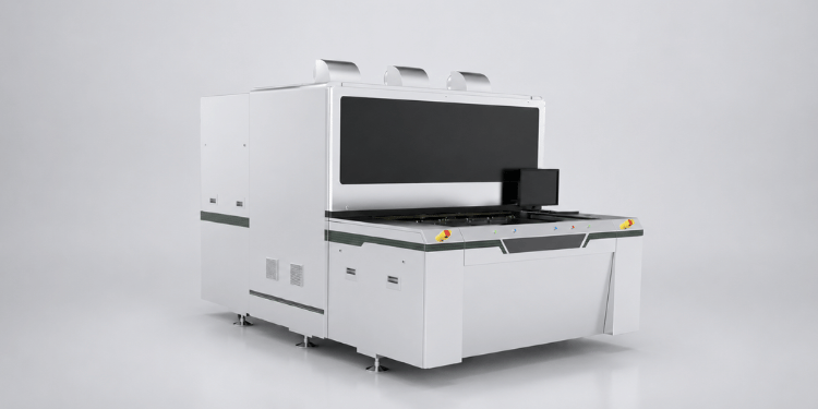
Laser direct imaging for high-precision PCB inner layer patterning
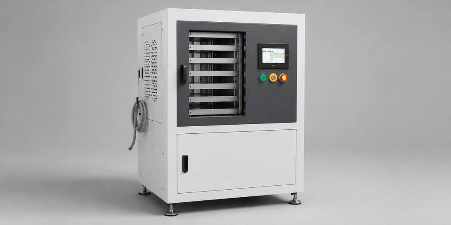
Multilayer PCB lamination press for bonding inner cores and prepregs under heat and pressure
Alumina ceramic delivers cost stability for mass production. AlN features superior thermal performance but comes with higher material and processing costs, suitable only for high-end extreme heat-flux projects.
Leave your contact information and project details, we will contact you ASAP!