
SMT Line
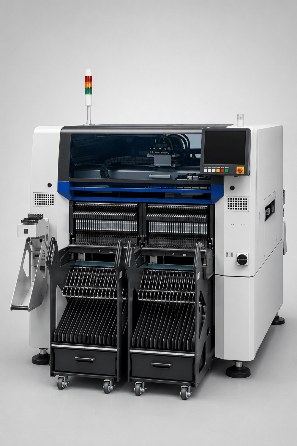
High-speed SMT assembly for fine-pitch components
Capacity 45K CPH

Low-Dk/Df Materials
Stable low-loss substrates minimize high-frequency signal attenuation.
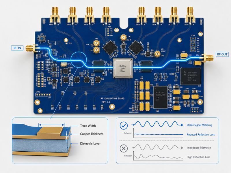
Precise Impedance Control
Tight tolerance calibration ensures accurate RF impedance matching.
Custom RF Fabrication
Deliver reliable prototyping and mass production for high-frequency PCBs.
Submit your RF stack-up and impedance requirements, and our engineering team provides DFM optimization and low-loss customized PCB solutions.
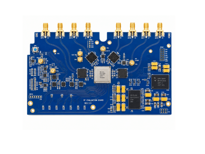
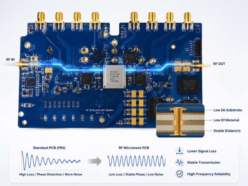
RF & Microwave PCB is a specialized high-frequency circuit board designed for radio frequency and microwave signal transmission. Different from standard FR4 PCBs, it uses low-loss dielectric materials and ultra-precision fabrication processes to reduce insertion loss, return loss and signal phase distortion.
Uses low Dk/Df substrates to maintain minimal signal attenuation and stable transmission at GHz-level high frequencies.
Strict line width and layer thickness tolerance ensures accurate impedance matching for RF antenna, filter and transceiver circuits.
Uniform lamination and material flatness prevent frequency offset and signal deviation in high-frequency working scenarios.
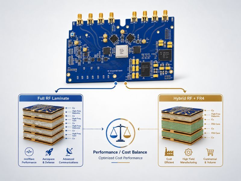
Graded low-loss stack structures for different frequency bands, from general RF to high-precision microwave applications.
Classic 2-layer microstrip structure with top RF signal traces and full bottom ground plane. It adopts uniform low-loss dielectric, delivering basic stable impedance performance for general low-to-medium frequency RF circuits.
Bluetooth modules, Wi-Fi 2.4G/5G circuits, ordinary IoT wireless boards
Stable high-frequency performance to support low-loss, high-precision wireless communication systems.
Standard mass-production specs and advanced high-end limits for high-frequency and millimeter-wave PCB fabrication.
 Capability Spec |  Standard RF PCB (Consumer & General Industrial) |  Advanced Microwave PCB (High-Frequency & Millimeter-Wave) |
|---|---|---|
| Min. Trace / Space | 4/4 mil | 3/3 mil |
| Supported Frequency Range | DC – 6GHz (Wi-Fi, Bluetooth, 4G LTE) | DC – 40GHz+ (5G Sub-6G, Millimeter-wave, Radar) |
| Matched Stack Structures | Single-sided microstrip, 4-layer symmetric stripline stacks | Multi-ground isolated microwave & hybrid high-frequency custom stacks |
| Max Total Layer Count | 6 Layers | 12 Layers |
| Impedance Control Tolerance | ±5% (Commercial RF Standard) | ±3% (Ultra-Precision Microwave Grade) |
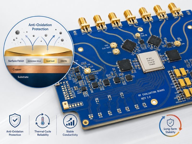
| Available Surface Finishes | OSP, ENIG | ENIG, Immersion Silver, Hard Gold (Low-Roughness RF Grade) |
| High-Frequency Substrates | Low-loss commercial FR4, entry-level RF laminates | Rogers, Isola, Teflon (PTFE), ceramic-filled ultra-low-loss laminates |
Advanced production equipment supporting stable quality, capacity, and reliable delivery.
High-speed SMT assembly for fine-pitch components
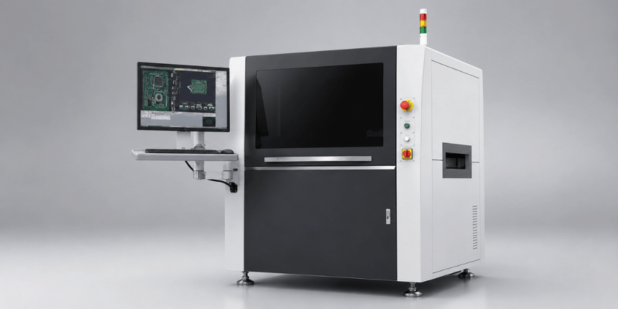
Automated visual inspection for defects
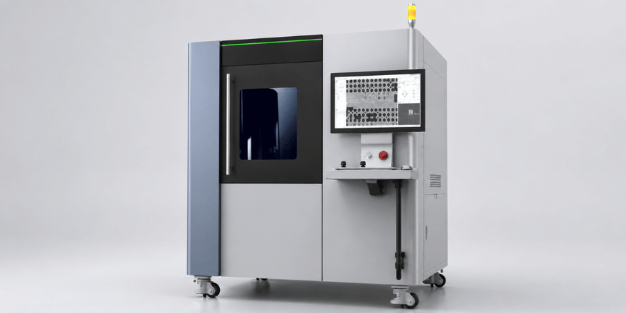
Non-destructive inspection for hidden solder joints
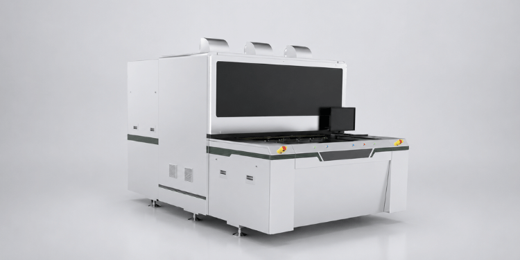
Laser direct imaging for high-precision PCB inner layer patterning
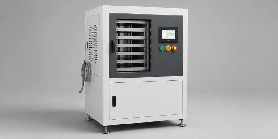
Multilayer PCB lamination press for bonding inner cores and prepregs under heat and pressure
Not necessarily. Low-loss FR4 works for low-frequency RF below 6GHz. 5G sub-6GHz and millimeter-wave circuits require Rogers, Isola or PTFE substrates to reduce high-frequency signal loss and phase shift.
Leave your contact information and project details, we will contact you ASAP!